Research Article | | Peer-Reviewed

Defect State Dynamics in Lead-Free Perovskite Solar Cells for Enhanced Efficiency

Received: 14 October 2024     Accepted: 4 November 2024     Published: 25 December 2024
Views:       Downloads:
Abstract

Perovskite photovoltaics have emerged as highly promising candidates for next-generation solar cells, achieving impressive power conversion efficiencies surpassing 22%, rivaling traditional silicon solar cells. Their advantages include lower manufacturing costs, tunable bandgaps, and potential for flexible, lightweight designs. However, the widespread use of lead (Pb) in perovskite absorbers raises significant environmental and health concerns. As a solution, researchers are exploring tin (Sn) as a non-toxic alternative due to its comparable electronic configuration, which may enable it to substitute lead without substantially compromising efficiency. In this study, SCAPS-1D software was employed to simulate lead-free tin-based perovskite solar cells, with a focus on analyzing how varying interface defect densities affect cell performance. Key cell parameters examined included the doping concentration of the perovskite absorption layer and the defect density within the perovskite bulk. Defect density is critical as it creates recombination centers that impede charge transport and decrease device efficiency. Findings from this simulation show that reducing defect density in the perovskite absorption layer notably improves overall cell performance, enhancing charge carrier mobility and reducing recombination losses. To further investigate interface effects, two specific interfaces were introduced: the TiO₂/perovskite interface, which serves as an electron transport layer, and the perovskite/hole transport material (HTM) interface. Analysis revealed that the TiO₂/perovskite interface plays a more substantial role in device performance, primarily due to its influence on carrier density and recombination rates, which are higher at this interface and critical in determining cell efficiency. Optimization of these parameters enabled the simulation of a device reaching a maximum efficiency of 24.63%. This research highlights the importance of interface engineering and defect management in tin-based, lead-free perovskite solar cells, demonstrating a feasible pathway toward environmentally sustainable, high-efficiency photovoltaics.

Published in International Journal of Materials Science and Applications (Volume 13, Issue 6)
DOI 10.11648/j.ijmsa.20241306.12
Page(s) 113-120
Creative Commons

This is an Open Access article, distributed under the terms of the Creative Commons Attribution 4.0 International License (http://creativecommons.org/licenses/by/4.0/), which permits unrestricted use, distribution and reproduction in any medium or format, provided the original work is properly cited.

Copyright

Copyright © The Author(s), 2024. Published by Science Publishing Group

Keywords

Simulation, Perovskite, Solar Cell, Efficiency

1. Introduction
Perovskite solar cells (PSCs) have gained significant attention in thin films solar cells since its inception especially by Kojima et al in 2009, organic inorganic hybrid perovskites have. This is because of its simple processing techniques and low cost of production than silicon based solar cells. These materials have exhibited excellent characteristics such as excellent transport properties , tunable band gap , high absorption coefficient, low temperature processing, direct band gap and longer diffusion lengths of charge carries.
Perovskite solar cells are considered to be one of the most potential solar cells in the near future. The major material used to harvest solar energy is the solar cell absorber, and perovskite have gained significant attention as the absorber layer. The power conversion efficiency (PCE) of CH3NH3PbX3 PSC has been significantly enhanced from 3.8% to 24.2% in 2016 .
With the massive improvement and contribution from perovskite solar cells to the photovoltaic world as whole, the use of lead (Pb) remains a major problem for mass production, and this is as a result of its environmentally unfriendly nature. Due to this, element Pb could be replaced by several elements which include bismuth (Bi) or antimony (Sb), where the perovskite displays a dimeric structure of A3B2X9 (e.g., (CH3NH3)3Bi2I9, Cs3Sb2I9) . Although these materials have realized full Pb-free, photovoltaic performance of their devices is so poor that these materials still need to be optimized , hence another suitable element to replace lead is tin (Sn). Although the toxicity and environmental effect of Sn are less studied, current data indicate that Sn is much easier to be removed from body (less than 400 days) than Pb, which has a long half-life of 20-30 years . Tin-based perovskite solar cells are still in the research phase and there are moderately limited publications on these solar cells compared to Pb-based PSC. This is as result of the instability of the 2+ oxidation state of tin (Sn2+) in methylammonium tin iodide (CH3NH3SnI3), which can be oxidized easily to a more stable Sn4+, and this process is called self-doping, where the Sn4+ acts as a p-dopant leading to the reduction in the solar cell efficiency. But in recent times, with the advancement in fabrication and encapsulation process, the stability of CH3NH3SnI3 based cells have been addressed by addition of SnF2 in the system to reduces the Sn4+ caused by the oxidation of Sn2+ . (HC(NH2)2SnI3 PSC with high duplicability has been fabricated with SnF2 as an inhibitor of Sn4+, and the encapsulated device has shown a steady performance for over 100 days, preserving 98% of its primary efficiency . Experimental and theoretical studies also show that CH3NH3SnI3 has a narrower band gap of 1.3 eV , which makes it possible to cover a wider range of the visible spectrum than that of Pb-based PSCs (1.55 eV). Also, this makes the tin perovskite absorber layer efficient with high optical properties and the widest light-adsorption range in all the CH3NH3BX3 (B = Sn, Pb; X = Cl, Br, I) compounds . CH3NH3SnI3 PSC with efficiency of over 20% have been obtained over years through simulation by optimizing basic parameters such as thickness of the absorber layer, doping concentration of the absorber layer etc.
An increase in Voc and Jsc’s of the cell signifies an overall improved performance of perovskite solar cells. The improved Jsc and Voc of the perovskite solar cell results in minimizing the interconnection losses of perovskite solar cells . Despite these cells having improved efficiencies and performance by varying its basic parameters as stated earlier, the solar cell materials tend to have defect states, which can affect the solar cells’ performance by decreasing its Jsc and Voc.
Jamal et. al. performed a numerical simulation on inverted planar structure perovskite solar cell based on NiO as a hole transport material (HTM). The effects of defect density and energy level of the perovskite absorber layer and perovskite/HTM interface layer on the performance of the solar cell was analysed, which revealed that values of Jsc, Voc, and FF of perovskite solar cells were significantly reduced with increasing the defect density of perovskite layer. The power conversion efficiency was also severely reduced from 25 to 5% when the defect density increased. As such defects states present in solar cells must be addressed to further improve the overall solar cell performance .
In this paper, the factors affecting the Pb-free CH3NH3SnI3 PSC efficiency with a detailed study of the effect of interface defect density are studied by one-dimensional device simulation using SCAPS-1D under AM1.5 illumination. The solar cell capacitance simulator (SCAPS) is a general solar cell simulation program that is based on three basic semiconductor equations and it is well adapted to the modeling of various hetero- and homo-junctions, multi-junction, and Schottky barrier devices.
2. Materials and Method
2.1. Cell Structure
The CH3NH3SnI3-based solar cell used has structure configuration of TCO glass substrate/TiO2 (electron transport material, ETM)/CH3NH3SnI3 (absorption layer)/ Spiro-OMeTAD (hole transport material, HTM)/metal back contact, and its schematic diagram was shown in Figure 1.
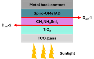
Figure 1. Schematic diagram of Sn-based Perovskite solar cell.
2.2. Initial Input Parameters
Material parameters are selected from experimental data and other theoretical results. The initial simulated parameters of the various layers are listed in Table 1 .
Table 1. Simulation parameters of Sn-based PSC.

Parameters

TCO

TiO2

CH3NH3SnI 3

Spiro-OMeTAD (HTM)

Thickness/nm

500

30

350

200

Band gap energy Eg /eV

3.5

3.2

1.3

3.17

Electron affinity χ/eV

4

4.0

4.17

2.6

Relative permittivity εr

9

9

8.2

3

Effective conduction band density Nc /cm 3

2.20×10 18

2.00×10 18

1.00×10 18

2.20×10 18

Effective valence band density Nv /cm −3

1.80×10 19

1.80×10 19

1.00×10 18

1.80×10 19

Electron mobility µn /(cm 2 /V·s)

20

20

1.6

2.00×10 −4

Hole mobility µp /(cm 2 /V·s)

10

10

1.6

2.00×10 −4

Donor concentration ND /cm −3

2.00×10 19

1.00×10 16

-

-

Acceptor concentration NA /cm −3

-

-

variable

2.00×10 19

Defect density Nt /cm −3

1.00×10 15

1.00×10 15

variable

1.00×10 15

Electron and hole thermal velocities of 107 cm/s were used. The defects in the perovskite absorption layer are set as neutral Gaussian distribution with a characteristic energy of 0.1 eV, and the defect energy level is at the center of band gap. The defects parameters simulated is shown in Table 2. To obtain absorption coefficient (α) curve, Aα of 105 is used and calculated by:
α=Aα(hνEg)1/2(1)
Table 2. Parameters setting of interface defect and the defect in the absorber.

Parameters

CH3NH3SnI3

ETM/CH3NH3SnI3 interface

CH3NH3SnI3/HTM interface

Defect type

neutral

neutral

neutral

Capture cross section for electrons and holes /cm2

2.0×10 −14

2.0×10 −14

2.0×10 −14

1.0×10 −15

1.0×10 −15

1.0×10 −15

Energetic distribution

Gaussian

single

single

Energy level with respect to Ev (above Ev) /eV

0.65

0.6

0.6

Characteristic energy /eV

0.1

-

-

Total density /cm −3

variable

variable

variable

2.3. Simulated Parameters
In this paper, we focused on the influence of doping concentration, the defect density of the perovskite absorber layer, and on the interface defect density between the Tin based perovskite layer and the ETM as well HTM. Defect density, Nt of 4.5×1017 cm−3 is initially set for the absorber layer. Tin perovskite displays a p-type conducting behavior because of the self-doping process as stated initially with Sn2+ easily oxidizing to Sn4+. The absorber layer is therefore simulated as the acceptor layer semiconductor with a carrier density of 3.2×1015 cm-3.
3. Results and Discussion
The perovskite layer thickness is set at 350 nm, some basic parameters of the cell structure, such as doping concentration of the perovskite layer, defect density of the perovskite layer are simulated initially to observe how they affect the general performance of the cell and with the optimized values of these parameters attained, the effect of interface defect density is simulated to further investigate its effects on the cell efficiency. With the initial values from Table 1, the current density-voltage characteristics was simulated, with the cell performance being low with open-circuit voltage (Voc) of 0.65 V, short-circuit current (Jsc) of 15.291 mA/cm2, fill factor (FF) of 41.57% and efficiency(η) of 4.13%
Firstly, the doping concentration of the absorber layer is simulated to observe its effect on the solar cell. The doping concentration of the perovskite layer is varied from 1014 cm-3 to 1019 cm-3 as seen below in Fig. 2. The efficiency of the cell structure increases as the NA value increases, at 2×1016 cm-3, efficiency of the cell reaches high value of 7.712% and decreases as the NA value exceeds 2×1016 cm-3.
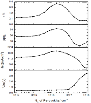
Figure 2. Variation of NA of perovskite layer with cell performance parameters.
It can also be observed that Voc increases with an increase in NA. Jsc increases as NA increases and attains a maximum value at 2×1016 cm-3 and further decreases rapidly as the NA value increases. The fill factor increases as NA increases. An appropriate value of NA is beneficial to for the enhancement of the photo-absorption efficiency as well as Jsc. The differences in the cell performance with respect to NA can be attributed to the built-in electric field and this is enhanced when doping concentration is increased, causing carrier separation, hence improving the general performance of the solar cell. Further increasing the NA above 1×1018 cm-3 decreases the cell performance due to higher Auger recombination rate. An increase in the recombination rate affects the cell performance greatly and should be avoided effectively. Results from Fig 3. corresponds with variation of NA results explained above in terms of quantum efficiency. At an optimum value of 2×1016cm-3, a higher cell performance is observed with the efficiency of the cell at 7.712%, Jsc of 18.94 mA/cm2, Voc of 0.706V and fill factor of 57.64% as compared to the initial doping concentration.
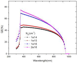
Figure 3. QE variation with NA of perovskite layer.
Next, the effect of defect density of the perovskite layer is simulated to observe its influence on the cell performance. The defect density (Nt) is varied from 1×10¹⁵ to 1×1019 cm-3. To have a better understanding of defect density effect on the performance of the cell and to reach a maximum cell efficiency, we need to consider generation and recombination process within the absorber layer. Photo-generated carriers (electron and holes) are generated on the absorber layer when the cell is illuminated by sunlight, causing the photogenerated carriers to be effectively separated and collected by the electrode and transfer towards an external current. Large number of carries are likely to be lost during this process if the perovskite layer quality is poor. Thus, causing higher recombination rate at higher defect density. Diffusion length and carrier lifetime of the charged carriers are also reduced due to the poor quality of the absorber layer, having a higher defect density with higher recombination rates. Shockley–Read–Hall recombination model (SRH) explains this effect of defect density of the perovskite layer on cell performance in equation (2).
R=ϑσn σn NT [np-ni2σP p+p1+σn[n+n1](2)
Where NT is number of defects per volume, ϑ is electron thermal velocity, σ and σ are capture cross-sections for electrons and holes, ni intrinsic number density, p1 and n1 are the concentrations of holes and electrons in valence band and trap defect, respectively n & p are the concentrations of electron and hole at equilibrium. From equation (2) that defect density is directly proportional to recombination (SRH).
As shown in Figure 4, the performance of the device is enhanced meaningfully with the reduction of Nt in the perovskite layer, and this is similarly observed with the numerical simulation of the lead perovskites cells . The device attained improved cell performance; Jsc of 30.8607 mA/cm2, Voc of 0.9872V, FF of 80.14% and efficiency of 24.05%.
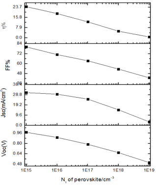
Figure 4. Variation of Nt of perovskite layer with cell performance parameters.
From equation (2), Nt is directly proportional to SRH, therefore, improvement of the cell performance can be attributed to a reduced recombination rate of the charged carriers as Nt is reduced. Further simulation was conducted with lower values of Nt such as 1×1014 cm-3 and an improved efficiency was observed but the inception of these values experimentally is difficult to achieve. Thus, Nt value of 1×1015 cm-3 was used.
As stated earlier, effect of defect density on carrier diffusion length is critical to the cell performance due to recombination. With a large defect density value, there is an increased rate of recombination which causes a reduced diffusion length of charge carriers and ultimately leading to a decreased carrier lifetime. Hence, lower defect density values are required since carrier lifetime is inversely proportional to defect density and diffusion length is directly proportional to carrier lifetime as shown in equation (3) and (4), respectively.
τn=1Ntυth (3)
Here, δ, υth, and Nt represents the capture cross-section area for electrons and holes, thermal velocity of carriers, and defect density, respectively.
LD = μe,hRTq τn,p(4)
LD, μ(e,h), and τn,p is the diffusion length, the electron and hole mobility, and the carrier lifetime, respectively.
This similar phenomenon was reported by Du et al., where lower Nt values give a longer diffusion length and a lower recombination rate which is recommended for an overall improved cell performance.
Finally, the effect of the interface defect density (Dint) on the cell performance was investigated. The junction quality of interface layers is very important to cell performance and should be considered with great importance because defects can reduce quality and cause high levels of recombination. In this paper, two interface defects are considered, with the interface defect 1 (Dint-1) inserted between the ETM and the absorber layer (TiO2/perovskite) and interface defect 2 (Dint-2) inserted between the absorber layer and HTM (perovskite/HTM). The Dint values are simulated between 1013 cm-3 to 1021 cm-3. It can be observed that with an increase in the Dint value, the cell performance reduces, showing that lower Dint values are beneficial to the cell’s performance. From Figure 5(a-c), it can be observed that Dint-1 has a significant effect on the cell performance. When Dint-1 increased from 1×10¹³ to 1×1016 cm-2, the cell efficiency decreases slightly and remains saturated at 1×1016 cm-2, as shown in Figure 5(c).
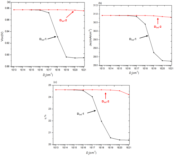
Figure 5. Variation of Dint-1 and Dint-2 layer with cell performance parameters. (a) Voc, (b) Jsc, and (c) efficiency.
The cells efficiency exhibited a reduction from 24.625% to 20.376% with the increase of Dint-1 from 1×10¹³ to 1×1021 cm-2. The influence of Dint-1 on the Voc was similar to that on the efficiency. The Jsc decreased (Δ≈8.626%) from 30.916 mA/cm2 to 28.249 mA/cm2, when Dint-1 increases from 1×10¹³ to 1×1021 cm-2. Voc of the cell structure shows a similar behavior as that of Jsc as seen in Figure 5(b). It can also be seen clearly in Figure 5(a-c) that, Dint-2 has a lower impact or effect on the cell performance as compared to Dint-1 with minimal value changes of Jsc, Voc, and efficiency. A higher defect density of the two interfaces brings about more traps and recombination centers and this affects the cell performance negatively. The massive influence and different effect from both interface defect density is caused by a high probability of photogenerated carriers been collected, such that photogenerated carriers absorbed is done at the p-n junction of the device thus generating more photocurrent. As such if the photogenerated carrier is generated at a distance from the p-n junction and more than a diffusion length, then possibility of carrier generated to be collected and transferred will be low, likewise the recombination rate will also be increased if the photogenerated carrier is generated closer to the surface of the cell structure. Also, for the perovskite absorber with a high absorption coefficient, the number of photogenerated electron-hole pairs at the side of the cell structured illuminated with light is higher than that of the dark side (not radiated) of the cell structure. Thus, as sunlight is illuminated towards TiO2/perovskite side of the cell structure, excess carrier density is generated, which leads to a larger recombination rate than at perovskite/HTM due the presence of localized recombination sites. Thus, the interface defect at TiO2/perovskite has stronger influence on device performance than perovskite/HTM.
The dependence of the interface defect states-1 (Dint-1) on band bending is shown in Figure 6(a) and (b). With Dint -1 higher than 11015 cm-2, the band bending shows an outward cliff thus, affecting the photo-generated electron flow, which leads to a decrease in VOC, as shown in Figure 5(a).
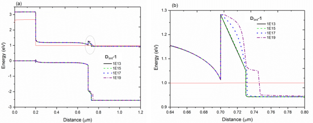
Figure 6. (a) Band Bending of cell with different Dit-1 value, (b) circled portion of Figure 6(a).
With the further increase of Dint -1, the reduction of the band bending is obviously enhanced, leading to a further decrease in VOC. However, for the Dint-1 values between 11013 and 11015 cm-2, the band bending shows a steep electron barrier cliff which allows for easy flow of the photo-generated electron, leading to a slight increase in VOC. Considering the influences of both interface defect states, the optimal efficiency for the Sn based perovskite solar cell is 24.63%, Jsc of 30.92 A/cm2, Voc of 0.98 eV and FF of 81.49% with the optimum simulated values of Dit-1 and Dit-2 being 11013 cm-2.
4. Conclusion
SCAPS simulation software is used to simulate lead-free CH3NH3SnI3 PSCs with diverse parameters are examined. The results show that to have a perovskite solar cell with improved efficiency, an appropriate carrier doping concentration of the Sn-perovskite is important, because it enhances the built-in electric field. Excess concentration also reduces the performance of the solar cell because of higher recombination rates. Nt of the perovskite is significant for high efficiency of solar cell. It was observed that with a density concentration of 1×1015 cm-3, the cell performance is increased with an efficiency increase from 7.71% to 24.05%. When Dint was considered, the cell performance reduces as Dint increases, with Dint-1 having a significant influence on the cell performance as compared to Dint-2. An optimum cell efficiency of 24.63% was obtained by optimizing simulation factors. The results attained shows that CH3NH3SnI3 PSCs are important with the possibilities of higher efficiency.
Acknowledgments
Thanks to Professor Marc Burgelman, of University of Gent for giving us the opportunity to use the SCAPS-1D software. This work was supported by the Zhejiang Provincial Natural Science Foundation of China (No. LY17F040001).
Author Contributions
Louis Oppong-Antwi: Conceptualization, Data curation, Formal Analysis, Investigation, Methodology, Software, Visualization, Writing – original draft, Writing – review & editing
Shihua Huang: Conceptualization, Supervision, Writing – review & editing
Conflicts of Interest
The authors declare no conflicts of interest.
References
[1] S. Bansal and P. Aryal, “Evaluation of new materials for electron and hole transport layers in perovskite-based solar cells through SCAPS-1D simulations,” 2017 IEEE 44th Photovolt. Spec. Conf. PVSC 2017, no. Idl, pp. 1–4, 2017,
[2] B. V. Lotsch, “New light on an old story: Perovskites go solar,” Angew. Chemie - Int. Ed., vol. 53, no. 3, pp. 635–637, 2014,
[3] Z. Wei, H. Chen, K. Yan, and S. Yang, “Inkjet printing and instant chemical transformation of a CH3NH3PbI3/nanocarbon electrode and interface for planar perovskite solar cells,” Angew. Chemie - Int. Ed., vol. 53, no. 48, pp. 13239–13243, 2014,
[4] M. J. P. Alcocer, T. Leijtens, L. M. Herz, A. Petrozza, and H. J. Snaith, “Electron-Hole Diffusion Lengths Exceeding Trihalide Perovskite Absorber,” Science (80-)., vol. 342, no. October, pp. 341–344, 2013,
[5] J. H. Noh, S. H. Im, J. H. Heo, T. N. Mandal, and S. Il Seok, “Chemical management for colorful, efficient, and stable inorganic-organic hybrid nanostructured solar cells,” Nano Lett., vol. 13, no. 4, pp. 1764–1769, 2013,
[6] G. Xing, N. Mathews, S. S. Lim, Y. M. Lam, S. Mhaisalkar, and T. C. Sum, “Long-Range Balanced Electron- and Hole-Transport Lengths in Organic-Inorganic CH 3 NH 3 PbI 3,” vol. 6960, no. October, pp. 498–500, 2013.
[7] D. Wang, H. Tao, X. Zhao, M. Ji, and T. Zhang, “Enhanced photovoltaic performance in TiO2/P3HT hybrid solar cell by interface modification,” J. Semicond., vol. 36, no. 2, 2015,
[8] A. F. Bouhdjar, L. Ayat, A. M. Meftah, N. Sengouga, and A. F. Meftah, “Computer modelling and analysis of the photodegradation effect in a-Si:H p-i-n solar cell,” J. Semicond., vol. 36, no. 1, pp. 0–8, 2015,
[9] J. Liu, S. Huang, and L. He, “Simulation of a high-efficiency silicon-based heterojunction solar cell,” J. Semicond., vol. 36, no. 4, pp. 1–8, 2015,
[10] M. A. Green, E. D. Dunlop, D. H. Levi, J. Hohl-Ebinger, M. Yoshita, and A. W. Y. Ho-Baillie, “Solar cell efficiency tables (version 54),” Prog. Photovoltaics Res. Appl., vol. 27, no. 7, pp. 565–575, 2019,
[11] M. Saliba et al., “Cesium-containing triple cation perovskite solar cells: Improved stability, reproducibility and high efficiency,” Energy Environ. Sci., vol. 9, no. 6, pp. 1989–1997, 2016,
[12] B. W. Park, B. Philippe, X. Zhang, H. Rensmo, G. Boschloo, and E. M. J. Johansson, “Bismuth Based Hybrid Perovskites A3Bi2I9 (A: Methylammonium or Cesium) for Solar Cell Application,” Adv. Mater., vol. 27, no. 43, pp. 6806–6813, 2015,
[13] Y. Li et al., “50% Sn-Based Planar Perovskite Solar Cell with Power Conversion Efficiency up to 13.6%,” Adv. Energy Mater., vol. 6, no. 24, pp. 1–7, 2016,
[14] A. Babayigit, A. Ethirajan, M. Muller, and B. Conings, “Toxicity of organometal halide perovskite solar cells,” Nat. Mater., vol. 15, no. 3, pp. 247–251, 2016,
[15] S. J. Lee et al., “Fabrication of Efficient Formamidinium Tin Iodide Perovskite Solar Cells through SnF2-Pyrazine Complex,” J. Am. Chem. Soc., vol. 138, no. 12, pp. 3974–3977, 2016,
[16] Y. Takahashi et al., “Charge-transport in tin-iodide perovskite CH3NH 3SnI3: Origin of high conductivity,” Dalt. Trans., vol. 40, no. 20, pp. 5563–5568, 2011,
[17] M. H. Kumar et al., “Lead-free halide perovskite solar cells with high photocurrents realized through vacancy modulation,” Adv. Mater., vol. 26, no. 41, pp. 7122–7127, 2014,
[18] N. K. Noel et al., “Lead-free organic-inorganic tin halide perovskites for photovoltaic applications,” Energy Environ. Sci., vol. 7, no. 9, pp. 3061–3068, 2014,
[19] P. Umari, E. Mosconi, and F. De Angelis, “Relativistic GW calculations on CH3 NH3 PbI 3 and CH3 NH3 SnI3 Perovskites for Solar Cell Applications,” Sci. Rep., vol. 4, pp. 1–7, 2014,
[20] C. C. Stoumpos, C. D. Malliakas, and M. G. Kanatzidis, “Semiconducting tin and lead iodide perovskites with organic cations: Phase transitions, high mobilities, and near-infrared photoluminescent properties,” Inorg. Chem., vol. 52, no. 15, pp. 9019–9038, 2013,
[21] Q. Y. Chen, Y. Huang, P. R. Huang, T. Ma, C. Cao, and Y. He, “Electronegativity explanation on the efficiency-enhancing mechanism of the hybrid inorganic-organic perovskite ABX3 from first-principles study,” Chinese Phys. B, vol. 25, no. 2, pp. 1–6, 2015,
[22] F. Si, F. Tang, H. Xue, and R. Qi, “Effects of defect states on the performance of perovskite solar cells,” J. Semicond., vol. 37, no. 7, p. 072003, 2016,
[23] Z. Xu and D. B. Mitzi, “SnI42--based hybrid perovskites templated by multiple organic cations: Combining organic functionalities through noncovalent interactions,” Chem. Mater., vol. 15, no. 19, pp. 3632–3637, 2003,
[24] J. Wang, H. Gao, J. Zhang, F. Meng, and Q. Ye, “Investigation of an a-Si/c-Si interface on a c-Si(P) substrate by simulation,” J. Semicond., vol. 33, no. 3, 2012,
[25] M. S. Jamal et al., “Effect of defect density and energy level mismatch on the performance of perovskite solar cells by numerical simulation,” Optik (Stuttg)., vol. 182, no. December 2018, pp. 1204–1210, 2019,
[26] U. Mandadapu, “Simulation and Analysis of Lead based Perovskite Solar Cell using SCAPS-1D,” Indian J. Sci. Technol., vol. 10, no. 1, pp. 1–8, 2017,
[27] T. Minemoto and M. Murata, “Device modeling of perovskite solar cells based on structural similarity with thin film inorganic semiconductor solar cells,” J. Appl. Phys., vol. 116, no. 5, 2014,
[28] H. J. Du, W. C. Wang, and J. Z. Zhu, “Device simulation of lead-free CH3NH3SnI3 perovskite solar cells with high efficiency,” Chinese Phys. B, vol. 25, no. 10, 2016,
[29] S. Huang, Z. Rui, D. Chi, and D. Bao, “Influence of defect states on the performances of planar tin halide perovskite solar cells,” J. Semicond., vol. 40, no. 3, 2019,
Cite This Article
  • APA Style

    Antwi, L. -. O., Huang, S. (2024). Defect State Dynamics in Lead-Free Perovskite Solar Cells for Enhanced Efficiency. International Journal of Materials Science and Applications, 13(6), 113-120. https://doi.org/10.11648/j.ijmsa.20241306.12

    Copy | Download

    ACS Style

    Antwi, L. -. O.; Huang, S. Defect State Dynamics in Lead-Free Perovskite Solar Cells for Enhanced Efficiency. Int. J. Mater. Sci. Appl. 2024, 13(6), 113-120. doi: 10.11648/j.ijmsa.20241306.12

    Copy | Download

    AMA Style

    Antwi L-O, Huang S. Defect State Dynamics in Lead-Free Perovskite Solar Cells for Enhanced Efficiency. Int J Mater Sci Appl. 2024;13(6):113-120. doi: 10.11648/j.ijmsa.20241306.12

    Copy | Download

  • @article{10.11648/j.ijmsa.20241306.12,
      author = {Louis - Oppong Antwi and Shihua Huang},
      title = {Defect State Dynamics in Lead-Free Perovskite Solar Cells for Enhanced Efficiency
    },
      journal = {International Journal of Materials Science and Applications},
      volume = {13},
      number = {6},
      pages = {113-120},
      doi = {10.11648/j.ijmsa.20241306.12},
      url = {https://doi.org/10.11648/j.ijmsa.20241306.12},
      eprint = {https://article.sciencepublishinggroup.com/pdf/10.11648.j.ijmsa.20241306.12},
      abstract = {Perovskite photovoltaics have emerged as highly promising candidates for next-generation solar cells, achieving impressive power conversion efficiencies surpassing 22%, rivaling traditional silicon solar cells. Their advantages include lower manufacturing costs, tunable bandgaps, and potential for flexible, lightweight designs. However, the widespread use of lead (Pb) in perovskite absorbers raises significant environmental and health concerns. As a solution, researchers are exploring tin (Sn) as a non-toxic alternative due to its comparable electronic configuration, which may enable it to substitute lead without substantially compromising efficiency. In this study, SCAPS-1D software was employed to simulate lead-free tin-based perovskite solar cells, with a focus on analyzing how varying interface defect densities affect cell performance. Key cell parameters examined included the doping concentration of the perovskite absorption layer and the defect density within the perovskite bulk. Defect density is critical as it creates recombination centers that impede charge transport and decrease device efficiency. Findings from this simulation show that reducing defect density in the perovskite absorption layer notably improves overall cell performance, enhancing charge carrier mobility and reducing recombination losses. To further investigate interface effects, two specific interfaces were introduced: the TiO₂/perovskite interface, which serves as an electron transport layer, and the perovskite/hole transport material (HTM) interface. Analysis revealed that the TiO₂/perovskite interface plays a more substantial role in device performance, primarily due to its influence on carrier density and recombination rates, which are higher at this interface and critical in determining cell efficiency. Optimization of these parameters enabled the simulation of a device reaching a maximum efficiency of 24.63%. This research highlights the importance of interface engineering and defect management in tin-based, lead-free perovskite solar cells, demonstrating a feasible pathway toward environmentally sustainable, high-efficiency photovoltaics.
    },
     year = {2024}
    }
    

    Copy | Download

  • TY  - JOUR
    T1  - Defect State Dynamics in Lead-Free Perovskite Solar Cells for Enhanced Efficiency
    
    AU  - Louis - Oppong Antwi
    AU  - Shihua Huang
    Y1  - 2024/12/25
    PY  - 2024
    N1  - https://doi.org/10.11648/j.ijmsa.20241306.12
    DO  - 10.11648/j.ijmsa.20241306.12
    T2  - International Journal of Materials Science and Applications
    JF  - International Journal of Materials Science and Applications
    JO  - International Journal of Materials Science and Applications
    SP  - 113
    EP  - 120
    PB  - Science Publishing Group
    SN  - 2327-2643
    UR  - https://doi.org/10.11648/j.ijmsa.20241306.12
    AB  - Perovskite photovoltaics have emerged as highly promising candidates for next-generation solar cells, achieving impressive power conversion efficiencies surpassing 22%, rivaling traditional silicon solar cells. Their advantages include lower manufacturing costs, tunable bandgaps, and potential for flexible, lightweight designs. However, the widespread use of lead (Pb) in perovskite absorbers raises significant environmental and health concerns. As a solution, researchers are exploring tin (Sn) as a non-toxic alternative due to its comparable electronic configuration, which may enable it to substitute lead without substantially compromising efficiency. In this study, SCAPS-1D software was employed to simulate lead-free tin-based perovskite solar cells, with a focus on analyzing how varying interface defect densities affect cell performance. Key cell parameters examined included the doping concentration of the perovskite absorption layer and the defect density within the perovskite bulk. Defect density is critical as it creates recombination centers that impede charge transport and decrease device efficiency. Findings from this simulation show that reducing defect density in the perovskite absorption layer notably improves overall cell performance, enhancing charge carrier mobility and reducing recombination losses. To further investigate interface effects, two specific interfaces were introduced: the TiO₂/perovskite interface, which serves as an electron transport layer, and the perovskite/hole transport material (HTM) interface. Analysis revealed that the TiO₂/perovskite interface plays a more substantial role in device performance, primarily due to its influence on carrier density and recombination rates, which are higher at this interface and critical in determining cell efficiency. Optimization of these parameters enabled the simulation of a device reaching a maximum efficiency of 24.63%. This research highlights the importance of interface engineering and defect management in tin-based, lead-free perovskite solar cells, demonstrating a feasible pathway toward environmentally sustainable, high-efficiency photovoltaics.
    
    VL  - 13
    IS  - 6
    ER  - 

    Copy | Download

Author Information