Germanium-based perovskite solar cells have garnered significant interest within the scientific community due to their non-toxicity and excellent stability. However, their low conversion efficiency is an obstacle to their application and design. We designed a device with a normal configuration structured as Glass / FTO / SnO2 / IDL1 / CsGeI3 / IDL2 / Cu2O / Au to improve our germanium-based perovskite solar cell, designed The integration of interface defect layers IDL1 and IDL2 the reduction of recombination. The study revealed that these IDL1 and IDL2 layers play a crucial role in solar conversion performance. By adjusting the thickness, electron affinity and defect density of the IDL1 and IDL2 layers, the conversion efficiency of our device exceeds 19%. However, an increase in temperature in the environment can negatively affect the cell by decreasing its photovoltaic efficiency.
| Published in | International Journal of Materials Science and Applications (Volume 14, Issue 4) |
| DOI | 10.11648/j.ijmsa.20251404.13 |
| Page(s) | 134-143 |
| Creative Commons |
This is an Open Access article, distributed under the terms of the Creative Commons Attribution 4.0 International License (http://creativecommons.org/licenses/by/4.0/), which permits unrestricted use, distribution and reproduction in any medium or format, provided the original work is properly cited. |
| Copyright |
Copyright © The Author(s), 2025. Published by Science Publishing Group |
Perovskite, CsGeI3, IDL1, IDL2, PCE Performance
 ) emissions. According to estimates compiled by the global budget project, pollution will increase by 0.8% in 2024, or 37.4 billion metric tons, compared with 2023
  . We have chosen
  and
and 
 ) and hole transport material (
  ), respectively. Considering recombination and interface quality, we added defect interface layers (
  ,
,  )
)  (1)
(1)  (2)
(2)  (3)
(3)  and
and  between the ETL and the perovskite layer and between the perovskite layer and the HTL, to prevent interface recombination and make the bandgap structure more resistant.
  and
and  ) have been provided as they are taken as work functions with energy values of -4.4eV for

[3, 5, 10] |
[1, 18] |
[3, 5, 22] |
[5, 13] |
[3, 5, 22] |
[1, 11, 18] | |
|---|---|---|---|---|---|---|
Eg (eV) | 3.5 | 3.5 | 1.41 | 1.6 | 1.41 | 2.17 |
Χ (eV) | 4.0 | 4.0 | 4.17 | 4.0 | 4.17 | 3.2 |
| 9.0 | 9.0 | 8.2 | 18 | 8.2 | 7.1 |
| 10 | 10 | 1.6 | 20 | 1.6 | 80 |
| 20 | 20 | 1.6 | 20 | 1.6 | 2000 |
| 1.8 | 2.6 | 1 | 1 | 1 | 1 |
| 2.2 | 4.36 | 1 | 1 | 1 | 2.2 |
| 0 | 0 | 1. | 2. | 1. | 1. |
| 2. | 1. | 0 | 2. | 0 | 0 |
| 1 | 1 | 1 | 1 | 1 | 1 |
Thickness (nm) | 500 | 30 | 8 | 1000 | 8 | 1000 |
 , showing a decrease in density as voltage increases. The modeling provided a voltage value (
  ) of 0.98 V, a current density of 24.30 mA/cm², a fill factor of 78.67%, and finally a conversion efficiency from 18.79%. Figure 2b illustrates the external quantum efficiency, consisting of three parts: between 300 and 400nm indicating a growth phase of yield, from 400 to 700nm representing the highest phase of quantum yield, above 80%, and beyond 700nm, we note a drastic drop in the external quantum yield of our device. Figure 2c represents the energy bands, where illustrates the conduction band energy level, the Fermi level of electrons, that of holes, and the valence band. This graph shows that the gap between the conduction band level and the valence band level results in an electric field of approximately 2.11 V/µm. The conversion efficiency of the cell model can be improved by reducing recombination between the different layers. Therefore, we examine the impact of varying the parameters of the
  layers on the performance of the solar cells.
  ) between the electron transport layer (ETL) and the absorbing layer and (
  ) between the hole transport layer (HTL) and the
  layer. Given the significant impact of layer thickness on internal efficiency and carrier transport in perovskite-based solar cells, we felt it necessary to assess the contribution of varying layer
  thicknesses on the efficiency of our cell. We fixed a thickness range for
  varying between 0.001 to 0.01µm and for layer
  between 0.001 to 0.004µm. The simulation with these values allowed us to plot the trends of the electrical parameters. Figure 3a shows that increasing the thickness of layer
  results in a slight drop in voltage, whereas the drastic decrease in open circuit voltage is more noticeable with the increase in thickness of layer
  , dropping from 5.95 to 4.03V. This leads to a drop in the open-circuit voltage, if we take the difference between the two values indicated above, and it remains within the range of the band gap of our cell absorber. Therefore, the thickness of layer
  plays a major role in the open circuit voltage. Figure 3b represents current density as a function of
  thickness variation. We see that increasing the thickness of layer
  does not significantly influence the current density. Conversely, increasing the thickness of layer
  leads to an increase in current density from 24.26mA/cm² for an
  thickness of 0.001µm to 24.29mA/cm² for an
  value of 0.004µm. Therefore, layer
  has a dominant influence on current density. Figure 3c shows the increase in fill factor as a function of increasing
  layer thickness. A sufficient proof that the variation of the fill factor depends on theeVolution of the thicknesses of the
  layers. Figure 3d illustrates the conversion efficiency diagram of our device, where we can see that the
  under goes a slight decrease in its value with the increase in thickness of
  . Conversely, the drop in yield is accentuated with theeVolution of thickness of
  , which decreases its value from 19.06 to 18.87%. In summary, we can expect to achieve a better conversion efficiency of our device with thicknesses for the defect interface layers (
  and
and  ) of 0.001µm.
  and
and  were varied between a range of 4.12 and 4.17eV. Figure 4a shows that the variation of electron affinity in layer
  does not impact the open circuit voltage. However, increasing the electron affinity energy of layer
  causes a rapideVolution of
  . Therefore, the electron affinity level is more balanced in layer
  , which explains its dominant impact compared to layer
  . Figure 4b shows the current density according to the variation of electron affinity. We can see that the increase in electronic energy in layer
  leads to a drop in from almost 24.10 mA/cm² to 24.00 mA/cm². However, for layer
  , increasing its electron affinity results in an increase in current density. The effect is therefore more significant in layer
  . In the simulation, the best cell current density value is obtained with the layer and the layer for electron energy values of 4.12eV and 4.17eV respectively.
  . Conversely, the variation of the fill factor is more pronounced as a function of theeVolution of electron affinity in layer
  . We have seen a drastic reduction in the fill factor value from 29% for an affinity of 4.12eV to less than 24% with an affinity of 4.17eV for layer
  . Figure 4d shows that increasing electron affinity in layer
  does not have major consequences, allowing the consistency of the conversion yield of our cell to be maintained. The increase in conversion performance is simply due to the addition of electron affinity in layer
  . Therefore, increasing the electron affinity in layer
  , which makes the system more stable and reduces electronic transitions. Consequently, a balanced electron affinity level in layer
  , equivalent to 4.17eV, improves the cell efficiency to 18.50%.
  layers on the electrical parameters in the figure below. Figure 5a shows that the variation of defect density in layer
  does not have much impact on the open circuit voltage. However, increasing defects in layer
  causes a drop in the open circuit voltage
  . On the layer, for a defect rate of , we can see that the is at its smallest value. In Figure 5b, the decrease in current density is most noticeable when the defect rate present in the layer is between and . Beyond this value, the presence of a fault
  in the layer has no effect on the current density. Regarding layer
  , increasing the defect density leads to a decrease in current density in this layer. The effect of defects is more pronounced in layer
  than in layer
  . In Figure 5c, the fill factor is not significantly influenced by the increase in defect density in layer
  . Although there is a slight variation in the fill factor in graph 5.c, it is too small to be significant. We can see from this graph that the decrease in the cell's conversion efficiency is systematically linked to the existence of defects
  in the layers. The conversion efficiency of the cell decreases from 19.01% for a defect rate of to 18.47% when the defect rate present is . Figure 5d shows the variation of the conversion efficiency of our cell as a function of the increase in defects in the interface layers. We can see that the decrease in conversion efficiency of the cell is systematically linked to the injection of defects in the
  layers. The conversion efficiency thus drops from 19.01% for defects of to 18.47% for defects of . In summary, the analysis of Figure 5d reveals that the increase in defect density hampers the efficiency of carrier flow. It increases the probability of recombination of electron-hole pairs, especially in the layer
  , and consequently reduces the performance of the device.
  whatever the temperature used. Regarding the fill factor illustrated by Figure 6d, we note an increase in the fill factor between 300°K and 400°K, reaching its best value at 400°K, close to 80%. Beyond 400°K, the increase in temperature leads to a decrease in fill factor. In Figure 6e, we clearly observe that temperature has a negative effect on the efficiency of the solar cell's performance, which is explained by the fact that high temperatures lead to the destruction and volatility of certain components, as well as instability in the device.
  interface layer has a significant impact on the conversion efficiency of the device, as it promotes better electron transfer. Conversely, the electron affinity affects the cell's conversion efficiency more when the
  layer takes an energy value of 4.17eV. The injection of defects into or within the
  or
or  layer reduces the performance of the device. Increasing the defect density hampers the efficiency of carrier flow. It increases the probability of recombination of electron-hole pairs, especially in the
  layer. As the temperature increases, the study showed that the performance of the solar device decreases. This leads to an increase in internal defects and degradation, resulting in an increase in recombination in the cell.
 IDL | Defect Interface Layers |
HTL | Hole Transport Layer |
ETL | Electron Transport Layer |
| [1] | Alioune SOW, Saliou Seck, Mamadou Salif Mane, Amadou Ndiaye, Bachirou Ndiaye, El-Hadji Mamadou Keita, Babacar Mbow, and Cheikh Sene. Effects of Transport Window Layers on All-inorganic CsPbI3-xBrx Perovskites Based Solar Cells. American Journal of Energy Research, 2023, Vol. 11, No. 2, 93-99. |
| [2] | S. SECK, A. Sow, M. S. Mané, A. Ndiaye, E. M. Keita, B. Ndiaye, B. Mbow, and C. Sène. Modeling and Analysis of a Mixed Sn-Ge Lead Free Perovskite Based Solar Cells. American Journal of Energy Research, 2024, Vol. 12, No. 1, 1-7. |
| [3] | Xiangrui Menga, Tianhang Tanga, Ruitao Zhangb, Kaiyuan Liua, Wenhao Lia, Lan Yanga, Yubao Songc, Xinxia Maa, Zhihai Chenga, and Jiang Wu. Optimization of germanium-based perovskite solar cells by SCAPS simulation. Optical Materials, 128(2022), 112427. |
| [4] | Xiaohui Li, Jianyao Tang, Putao Zhang, and Shengjun Li. Strategies for achieving high efficiency and stability in carbon-based all-inorganic perovskite solar cells. Cell Reports Physical Science 5, 2024, 101842. |
| [5] | Junhua Lu, Shuo Chen, Hairong Wang, Long Qiu, Chenyu Wu, Wencan Qian, Zhijie Wang, Kai Huang, Jiang Wu, Huan Chen, and Yuxing Gao. Replacing the electron-hole transport layer with Doping: SCAPS simulation of lead-free germanium-based perovskite solar cells based on CsGeI3. preprint research paper has not been peer reviewed. Electronic copy available at: |
| [6] | M. Khalid Hossain, Mustafa K. A. Mohammed, M. Shihab Uddin, G. F. Ishraque Toki, Rahul Pandey, Md. Ferdous Rahman, D. P. Samajdar, Md. Rasidul Islam, JayaMadan, Sagar Bhattarai, H. Bencherif, Mongi Amamik and D. K. Dwivedil. Achieving above 24% efficiency with non-toxic CsSnI3 perovskite solar cells by harnessing the potential of the absorber and charge transport layers. RSC Adv., 2023, 13, 23514–23537. |
| [7] | Nurul Afiqah Buruhanutheen, Ahmad Sharmi Abdullah, Mohd Halim Irwan Ibrahim, Fauzan Ahmad and Mohd Haniff Ibrahim. Modeling of Germanium-Based Perovskite Solar Cell for Different Hole Transport Materials and Defect Density. PHOTONICS LETTERS OF POLAND, 2023, VOL. 15(3), 45-47. |
| [8] | Deepthi Jayan Ka, Varkey Sebastiana, and Joji Kurian. Simulation and optimization studies on CsPbI3 based inorganic perovskite solar cells. SolarEnergy, 2021, Vol 221, 99–108. |
| [9] | T. Jesper Jacobsson, WolfgangTress, Juan-Pablo Correa-Baena, Tomas Edvinsson, and Anders Hagfeldt. Room Temperature a sa Goldilocks Environment for CH3NH3PbI3 Perovskite Solar Cells: The Importance of Temperature on Device Performance. The Journal of Physical Chemistry, |
| [10] | Lipsa Rani Karna, Rohitash Upadhyay, and Avijit Ghosh. All‑inorganic perovskite photovoltaics for power conversion efficiency of 31%. Scientific Reports, (2023) 13: 15 212. |
| [11] | Abhijeet J. Kale, Rajneesh Chaurasiya, and Ambesh Dixit. Inorganic Lead-Free Cu2AuBiCL6 Perovskite Absorber and Cu2O Hole Transport Material Based Single-Junction Solar Cells with 22.18% Power Conversion Efficiency. Adv. Theory Simul. 2021, Vol 4, No 2000224, 1 of 14. |
| [12] | Isabel Mesquita, Luísa Andrade, and Adélio Mendes. Temperature Impact on Perovskite Solar Cells Under Operation. ChemSusChem, |
| [13] | Thirumal Krishnamoorthy, Hong Ding, Chen Yan, Wei Lin Leong, Tom Baikie, Ziyi Zhang, Matthew Sherburne, Shuzhou Li, Mark Asta, Nripan Mathews, and Subodh G. Mhaisalkar. Lead-free Germanium Iodide Perovskite Materials for Photovoltaic Application. J. Name., 2013, 00, 1-3. |
| [14] | Zhizai Li, Faguang Zhou, Qian Wang, Liming Ding b, and Zhiwen Jin. Approaches for thermodynamically stabilized CsPbI3 solar cells. Nano Energy, 2020, Vol 71, 104634. |
| [15] | Tian Luo, Yufan Xia, Jiawei Huang, Xi Huang, Zhenyuan Wu, Yuxuan Chen, Xin Xu, Weiguang Xie, Pengyi Liu, Cuiying Hu, Xing Lu and Tingting Shi. Different structuraleVolutions of inorganic perovskite CsGeI3. CrystEngComm, 2021, Vol 23, 4917. |
| [16] | Shambhavi Rai, B. K. Pandey, and D. K. Dwivedi. Modeling of highly efficient and low cost CH3NH3Pb(I1-xClx)3 based perovskite solar cell by numerical simulation. Optical Materials, 2020, Vol 100, 109631. |
| [17] | Carlos Pinzón, Nahuel Martínez, Guillermo Casas, Fernando C. Alvira, Nicole Denon, Gastón Brusasco, Hugo Medina Chanduví, Arles V. Gil Rebaza and Marcelo A. Cappelletti. Optimization of Inverted All-Inorganic CsPbI3 and CsPbI2Br Perovskite Solar Cells by SCAPS-1D Simulation. Solar 2022, 2, 559–571. |
| [18] | Lingyan Lin, Linqin Jiang, Ping Li, Hao Xiong, Zhenjing Kang, Baodian Fan, Yu Qiu. Simulated development and optimized performance of CsPbI3 based all-inorganic perovskite solar cells. Solar Energy, 2020, Vol 198, 454-460. |
| [19] | Nahuel Martínez, Carlos Pinzón, Guillermo Casas, Fernando Alvira, Marcelo Cappelletti. Computational study of inverted all-inorganic perovskite solar cells based on CsPbIxBr3-x absorber layer with band gap of 1.78eV. Accelerating the world's research, 2020. |
| [20] | Xin Wu, Yizhe Liu, Feng Qi, Francis Lin, Huiting Fu, Kui Jiang, Shengfan Wu, Leyu Bi, Deng Wang, Fang Xu, Alex K.-Y. Jen and Zonglong Zhu. Improved stability and efficiency of perovskite/ organic tandem solar cells with an all-inorganic perovskite layer. Journal of Materials Chemistry A, 2021. |
| [21] | Les Echos “ Les émissions mondiales de CO2 liées aux énergies fossiles vont battre un nouveau record cette année”. Available from: |
| [22] | Bingcheng Yu, Chuantian Zuo, Jiangjian Shi, Qingbo Meng, and Liming Ding, ‘‘Defect engineering on all-inorganic perovskite solar cells for high efficiency’’, Journal of Semiconductors, 2021, Vol 42, 050203. |
APA Style
Sow, A., Seck, S., Faye, M., Mane, M. S., Ndiaye, A., et al. (2025). Study of the Effect of Interface Defect Layers (IDL1 and IDL2) on CsGeI3 Perovskite Solar Cells by SCAPS 1D Simulation. International Journal of Materials Science and Applications, 14(4), 134-143. https://doi.org/10.11648/j.ijmsa.20251404.13
ACS Style
Sow, A.; Seck, S.; Faye, M.; Mane, M. S.; Ndiaye, A., et al. Study of the Effect of Interface Defect Layers (IDL1 and IDL2) on CsGeI3 Perovskite Solar Cells by SCAPS 1D Simulation. Int. J. Mater. Sci. Appl. 2025, 14(4), 134-143. doi: 10.11648/j.ijmsa.20251404.13
@article{10.11648/j.ijmsa.20251404.13,
  author = {Alioune Sow and Saliou Seck and Modou Faye and Mamadou Salif Mane and Amadou Ndiaye and Bachirou Ndiaye and Babacar Mbow and Cheikh Sene},
  title = {Study of the Effect of Interface Defect Layers (IDL1 and IDL2) on CsGeI3 Perovskite Solar Cells by SCAPS 1D Simulation
},
  journal = {International Journal of Materials Science and Applications},
  volume = {14},
  number = {4},
  pages = {134-143},
  doi = {10.11648/j.ijmsa.20251404.13},
  url = {https://doi.org/10.11648/j.ijmsa.20251404.13},
  eprint = {https://article.sciencepublishinggroup.com/pdf/10.11648.j.ijmsa.20251404.13},
  abstract = {Germanium-based perovskite solar cells have garnered significant interest within the scientific community due to their non-toxicity and excellent stability. However, their low conversion efficiency is an obstacle to their application and design. We designed a device with a normal configuration structured as Glass / FTO / SnO2 / IDL1 / CsGeI3 / IDL2 / Cu2O / Au to improve our germanium-based perovskite solar cell, designed The integration of interface defect layers IDL1 and IDL2 the reduction of recombination. The study revealed that these IDL1 and IDL2 layers play a crucial role in solar conversion performance. By adjusting the thickness, electron affinity and defect density of the IDL1 and IDL2 layers, the conversion efficiency of our device exceeds 19%. However, an increase in temperature in the environment can negatively affect the cell by decreasing its photovoltaic efficiency.},
 year = {2025}
}
TY  - JOUR
T1  - Study of the Effect of Interface Defect Layers (IDL1 and IDL2) on CsGeI3 Perovskite Solar Cells by SCAPS 1D Simulation

AU  - Alioune Sow
AU  - Saliou Seck
AU  - Modou Faye
AU  - Mamadou Salif Mane
AU  - Amadou Ndiaye
AU  - Bachirou Ndiaye
AU  - Babacar Mbow
AU  - Cheikh Sene
Y1  - 2025/07/31
PY  - 2025
N1  - https://doi.org/10.11648/j.ijmsa.20251404.13
DO  - 10.11648/j.ijmsa.20251404.13
T2  - International Journal of Materials Science and Applications
JF  - International Journal of Materials Science and Applications
JO  - International Journal of Materials Science and Applications
SP  - 134
EP  - 143
PB  - Science Publishing Group
SN  - 2327-2643
UR  - https://doi.org/10.11648/j.ijmsa.20251404.13
AB  - Germanium-based perovskite solar cells have garnered significant interest within the scientific community due to their non-toxicity and excellent stability. However, their low conversion efficiency is an obstacle to their application and design. We designed a device with a normal configuration structured as Glass / FTO / SnO2 / IDL1 / CsGeI3 / IDL2 / Cu2O / Au to improve our germanium-based perovskite solar cell, designed The integration of interface defect layers IDL1 and IDL2 the reduction of recombination. The study revealed that these IDL1 and IDL2 layers play a crucial role in solar conversion performance. By adjusting the thickness, electron affinity and defect density of the IDL1 and IDL2 layers, the conversion efficiency of our device exceeds 19%. However, an increase in temperature in the environment can negatively affect the cell by decreasing its photovoltaic efficiency.
VL  - 14
IS  - 4
ER  -
Department Physics, Faculty of Sciences and Technology, Semiconductors and Solar Energy Laboratory, Cheikh Anta DIOP University, Dakar, Senegal
Department Physics, Faculty of Sciences and Technology, Semiconductors and Solar Energy Laboratory, Cheikh Anta DIOP University, Dakar, Senegal
Department Physics, Faculty of Sciences and Technology, Semiconductors and Solar Energy Laboratory, Cheikh Anta DIOP University, Dakar, Senegal
Department Physics, Faculty of Sciences and Technology, Semiconductors and Solar Energy Laboratory, Cheikh Anta DIOP University, Dakar, Senegal
Department Physics, Faculty of Sciences and Technology, Semiconductors and Solar Energy Laboratory, Cheikh Anta DIOP University, Dakar, Senegal
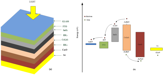
Figure 1. Structure of the cell (a) and energy diagram (b).
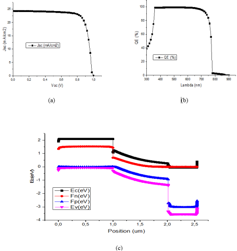
Figure 2. Current density as a function of voltage (a), external quantum efficiency (b), and energy band diagram (c).
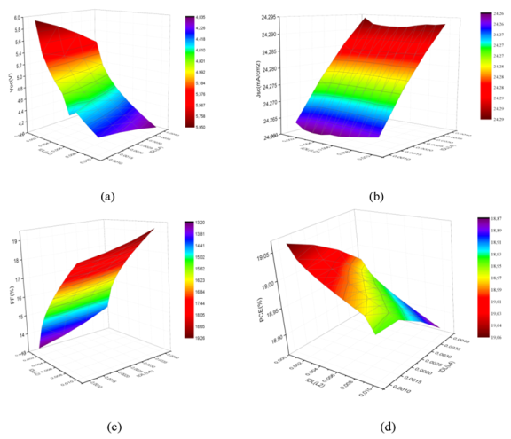
Figure 3. Effect of varying the thickness of interface defect layers: (a)![]() , (b)
, (b) ![]() , (c)
, (c) ![]() , and (d)
, and (d) ![]() .
.
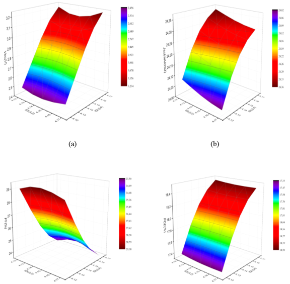
Figure 4. Impact of varying electron affinity of interface defect layers: (a)![]() , (b)
, (b) ![]() , (c) FF, and (d)
, (c) FF, and (d) ![]() .
.
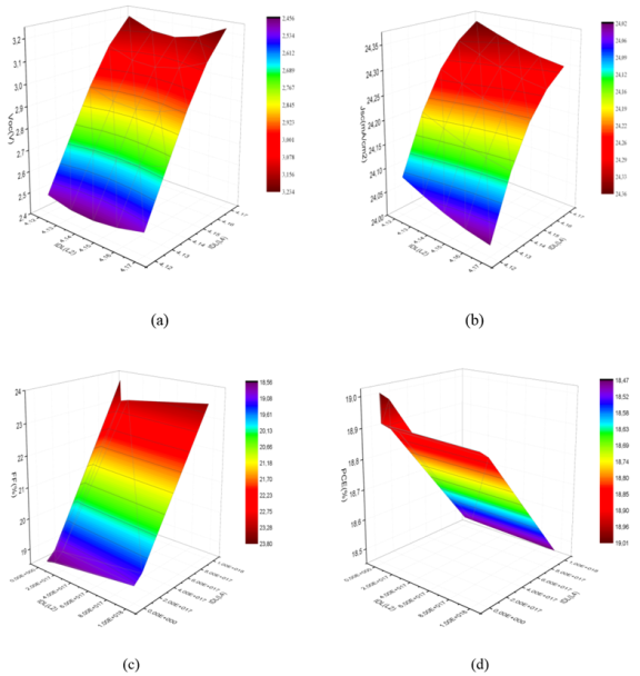
Figure 5. Impact of variation defect density of interface defect layers: (a) ![]() , (b)
, (b) ![]() , (c)
, (c) ![]() , and (d)
, and (d) ![]() .
.
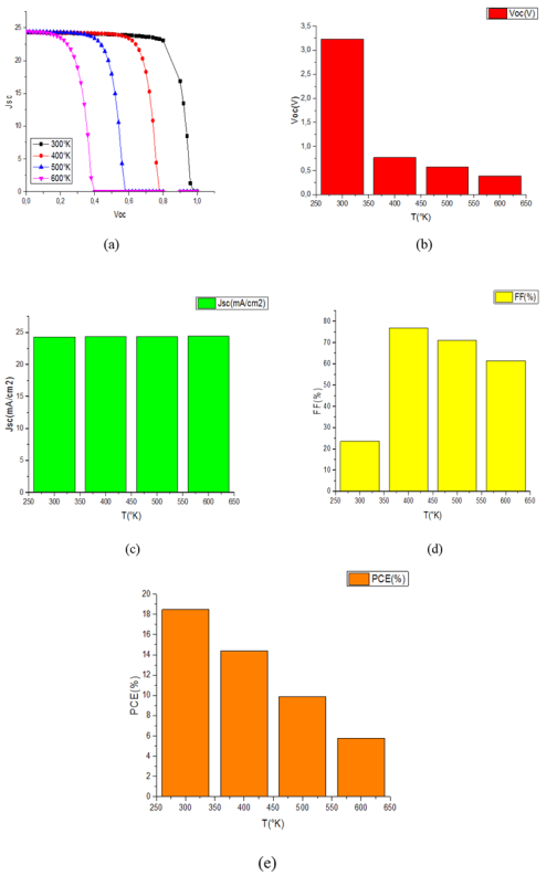
Figure 6. Effect of temperature on J-V characteristics (a) and electrical parameters: (b) ![]() , (c)
, (c) ![]() , (d)
, (d) ![]() , and (e)
, and (e) ![]() .
.